Loading...
 

NanoBlog

A blog about anything nanotech

Lab-on-chips webinar

morreale Tuesday 11 of December, 2012
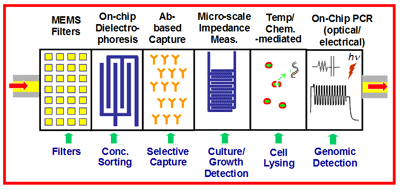
The IEEE hosted the Tech Insider: From Labs-on-Chips to Cellular Machines: Interfacing Engineering and Biology at the Micro and Nanoscale webinar today. Professor Bashir from the University of Illinois, Urbana-Champaign provided a very interesting presentation on architectures for labs-on-chips to address three grand challenges. These include:
  1. HIV/AID detection
  2. Diagnostics for cancer detection via miRNA
  3. Engineering of biological systems
Then Mark Winter from the X Prize Foundation describe the initiatives that the foundation is working on to promote point of use healthcare devices. The first is the Qualcom Tricorder X Prize and Nokia Sensing X Challenge which involve $10M and $2.5M in prizes respectively. The webinar should be on archive within a week.

Image

Plasma ALD webinar

morreale Thursday 22 of November, 2012
Oxford Instruments posted a archive of their Plasma ALD webinar. Professor Erwin Kessels describes the thermal ALD and Plasma ALD process steps. The process includes four generals steps.
  1. Precursor exposure
  2. Purge
  3. Reactant exposure
  4. Purge
Thermal ALD takes place at temperatures between 150 to 400°C. Using plasma ALD reduces deposition temperatures by 100-150°C. Many materials can be deposited at room temperature with fair to good characteristics. The four step process is repeated multiple times to build up a film layer-by-layer to the precise thickness desired. The reactants must produce a self-limiting reaction on the substrate surface to be considered ALD. The merits of plasma ALD include:
  • Improved material properties
  • Deposition at lower temperatures
  • Increased choice of precursors and materials
  • Good control of film stoichiometry and film composition
  • Increased growth rates
  • More process versatility generally
Plasma ALD challenges include
  • Reduced conformity or step coverage
  • Plasma induced damage (ion bombardment and UV damage)
  • Industrial scale up more complex
For more information, see Atomic layer deposition of nanostructured materials by professor Kessel, and Vacuum Science Technology A 29 050801 (2011) Profijt et. al.

The Twinkie guide to Nanotechnology

morreale Tuesday 20 of November, 2012
The Twinkie guide to Nanotechnology is a 25 minute presentation given by scientist Andrew Maynard on well you guessed it nanotechnology. The guide is part of the Project on Emerging Nanotechnology. Dr Maynard gives some sense of relative scale of the nanotechnology. A Twinkie at about 10 cm in scale and DNA at about 2 nm are the same relative size difference as the Moon and a Twinkie, for example. He is optimistic about the future of nanotechnology but perception is very important for public acceptance and care must be taken to make sure that nanotechnology is safe. Studies have shown that rats that breath nanoparticles accumulate the nanoparticle in their brains instead of in the lungs which is typical of larger particles.

2012 MRS Fall meeting streaming

morreale Thursday 15 of November, 2012
The 2012 MRS Fall meeting will stream some talks live from the Boston Convention center. The remaining talks will be available after the talk completes. Presentations include:
  • Selected Tutorial Sessions, Award and Plenary talks
  • Symposium G: Materials as Tools for Sustainability
  • Symposium L: Biomimetic Nanoscale Platforms, Particles, and Scaffolds for Biomedical Applications
  • Symposium W: Carbon Nanomaterials (with an emphasis on Graphene)
  • Symposium ZZ: Communicating Social Relevancy in Materials Science and Engineering Education

Be sure to register.

Image

DIY Nano App

morreale Thursday 15 of November, 2012
The Nanoscale Informal Science Education (NICE) Network has released the DIY Nano app for the iPhone. The app provides information on nanoscale science, engineering, and technology for the family at your finger tips. It received a silver honor award at iTunes.

Image

Nanotransistor course Oct 29, 2012

morreale Tuesday 09 of October, 2012
Don't forget that Professor Mark Lundstrom is offering a course on Nanotransistors starting October 29, 2012 and running for five weeks. His introduction video provides a good overview of transistors, and a summary of the course contents. There is a $30 fee to register and $225 fee to receive credit for the course.

Nano process database

morreale Saturday 29 of September, 2012
Internano is a resource for nanotechnology manufacturing, and has posted half a dozen or so open source manufacturing processes. The include:
  • Fabrication of a nanoporous template from a diblock copolymer film - electric field alignment
  • Fabrication of a nanoporous template from a diblock copolymer film - solvent annealing
  • Fabrication of a nanoporous template from a diblock copolymer film - neutral brush
  • Pulse-reversed electrodeposition with QCM monitoring to make magnetic nanowires in a nanotemplate
  • Heat-controlled size evolution of dodecanethiol-protected Au nanoparticles in the solid state
  • Phosphine-stabilized gold nanoparticles
  • Inkjet-printed graphene electronics
  • High-yield dielectrophoretic assembly of two-dimensional graphene nanostructures

Nano.gov webinar

morreale Thursday 20 of September, 2012
Nano.gov had a webinar today to discuss the sites resources and how that site might be improved. The speakers included:
  • Marlowe Epstein-Newman, National Nanotechnology Coordination Office (NNCO)
  • Carl Batt, Cornell University
  • Josh Chamot, National Science Foundation (NSF)
  • Mary Ann Latko, American Industrial Hygiene Association (AIHA)
  • Nazhin Beiramee, OMNI Studios
Most of the webinar involved discussions about the use of nano.gov, what and how user use the site, and what people want from the site. It was interesting to see how everyone seems to be working this issue regardless of the content. The site is built using Drupal which is an open source content management platform. Anyway, the panelist described several sites of interest:
  • nanooze.org is a nanotechnology website for kids.
  • GoodNanoGuide is a website for scientists and engineers looking for info on the industrial hygiene of nanomaterials.

GaAs nanowires grown on graphene

morreale Thursday 13 of September, 2012
Research at the Norwegian University of Science and Technology have grown GaAs nanowires on an epitaxial graphene layer using a MBE system. Ga is first deposited onto the graphene substrate and it forms nanoparticles that align with the graphene lattice. As is then introduce and the nanowires then grow without further catalysts. The nanowires form an array and are attached to the graphene substrate that is flexible and transparent. The details of the work can be found in Vertically Aligned GaAs Nanowires on Graphite and Few-Layer Graphene: Generic Model and Epitaxial Growth and can be seen in this interesting video.

Image