Loading...
 

NanoBlog

A blog about anything nanotech

Nanocrystalline Dye-Sensitized Solar Cell Kit

morreale Tuesday 17 of July, 2012
Greg P. Smestad, Ph.D. developed a prototype nanocrystalline dye sensitized solar cell kit in 1998, using dyes from plants and this kit is available from The Institute for Chemical Education (ICE) for $50. The Nanocrystalline Dye-Sensitized Solar Cell Kit is designed to to teach students how to fabricate a solar cell. Sol Ideas sold the kit previously, but still has some good directions, reference information, and links on their site. The dye is prepared from blackberries, raspberries, pomegranate seeds, Bing cherries, or green citrus leaves, fresh or frozen. There are a lot of items that are needed and are not in the kit so check out the list at the link on the ICE page.

Image

Plastic Logic displays

morreale Tuesday 17 of July, 2012
The BBC films a short segment about Plastic Logic's new flexible color display panels. The panels look pretty neat and should be available perhaps next year. The BBC shows some panels being made, but is short on the details. The longer production video shows panels being made and some cool automated fabrication equipment, but I could not find out anything useful about the materials used to make the organic transistors.

Nanosensors initiative

morreale Friday 13 of July, 2012
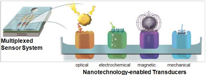
The NSI has started an initiative to help transition nanosensors to market by addressing concerns about their reliability, repeatability and robustness while also determining the potential hazards associated with nanomaterials in the environment. NSI has released a white paper describing the process and issues.

Image

Copper deposition system

morreale Wednesday 11 of July, 2012
Applied Materials has introduced the new the Applied Endura® Amber™ physical vapor deposition system. It was designed to deposit copper interconnects with dimensions of around 22 nm (200 atoms across). The system deposits a thin layer of copper and then warms it to allow capillary forces to pull the copper into the copper connection trenches. Electrochemical plating then follows to fill in this seed layer. A short video on Applied Materials Blog gives an overview of the new system.

Image

Nanoscale transistor course

morreale Wednesday 27 of June, 2012
The nanoHUB is offering a 5 week online course on Nanoscale transistors from October 29 to November 20, 2012. The course is taught by professor Mark Lundsrom at Purdue University. The registration fee is $30 or $225 with CEU credits. The topics include:
  • Week 1: The transistor—controlling current by modulating a barrier
  • Week 2: MOS electrostatics
  • Week 3: The ballistic nanotransistor
  • Week 4: The quasi-ballistic nanotransistor
  • Week 5: Practical and fundamental limits

Semiconductor special collection

morreale Monday 25 of June, 2012
IOP Science has posted a special collection on Semiconductors that is presently free to read. Topics include:
  • Photovoltaics, LEDs and devices
  • Quantum dots and quantum wells
  • Plasmonics and metamaterials
  • II-VI semiconductors
  • III-V semiconductors
  • IV semiconductors
  • Growth and synthesis
  • Lasers
  • Terahertz
  • Topical insulators
  • Thermal and electronic transport


Image

Photovoltaic Manufacturing Consortium

morreale Friday 15 of June, 2012
The Photovoltaic Manufacturing Consortium was started as part of the Department of Energy's Sunshot Initiative. The aim of the program is to bring together 40 companies to develop the packaging and manufacturing technology to bring the cost of solar panels down to $1/W. It is thought that this will make the US competitive and a world exporter of solar array technology.